Now that you understand why the hardware evolved this way, you can look at the DGX H100 and understand every design decision:
DGX H100 — anatomy and alternatives
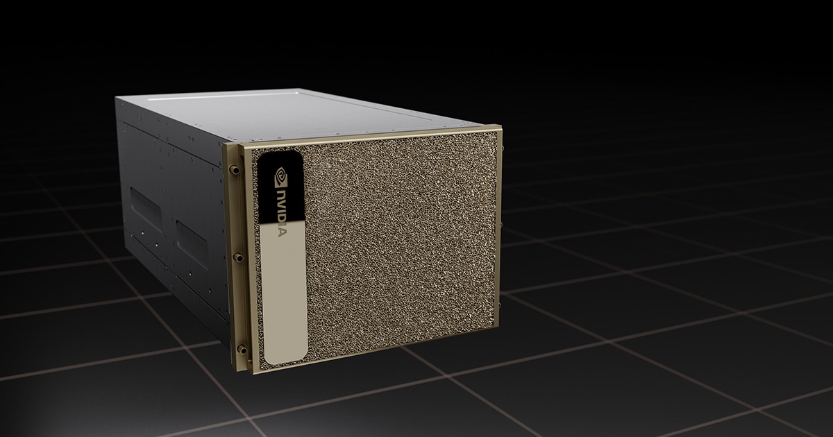
Figure: Official NVIDIA DGX H100 system image. Seeing the chassis itself helps ground the anatomy discussion in the physical box operators actually deploy.
Every choice in the DGX design is an answer to a specific constraint:
| Design decision | Why |
|---|---|
| 8 GPUs per chassis | Maximum NVLink bandwidth per GPU within practical power and thermal limits |
| 4 NVSwitch chips | Non-blocking all-to-all between 8 GPUs at 900 GB/s per GPU |
| 1 ConnectX-7 per GPU | No shared uplinks -- each GPU gets its own 400G path to the fabric |
| 8 NICs on 8 different switches | Rail topology -- fault isolation and maximum AllReduce performance |
| 2 Intel Xeon CPUs | Management only -- training is GPU + NIC, CPUs are mostly idle |
| 8x 3.84 TB NVMe U.2 (~30 TB) | Local OS, checkpointing -- training data lives on shared parallel storage (BeeGFS, WEKA) |